Bangle.js Technical Information
For general Bangle.js information, try the Bangle.js 1 or the Bangle.js 2 pages
This page contains detailed information on Bangle.js's 1's internals. Click here for Bangle.js 2. If you're just writing JS then you should have no need for this information, but if you plan on modifying the Bangle.js firmware it might be of interest.
Contents
Features
- IP68 Waterproof (everyday use, not swimming or baths)
- Nordic 64MHz nRF52832 ARM Cortex-M4 processor with Bluetooth LE
- 64kB RAM 512kB on-chip flash, 4MB external flash
- 1.3 inch 240x240 16 bit LCD display with 2 zone touch
- GPS/Glonass receiver (UBlox)
- Heart rate monitor
- 3 Axis Accelerometer (with Pedometer and Tap detect)
- 3 Axis Magnetometer
- Vibration motor
- 350mAh battery, 1 week standby time
- 5 x 5 x 1.7 cm case, plastic with stainless steel ring
- Can be disassembled with just 4 screws
Software
Where mentioned in the source code or filenames, Q3 references Bangle.js 2, and F18 references Bangle.js 1.
The Espruino version for Bangle.js has a few specific modifications:
jswrap_bangle.ccontains allBangle.*functions and pretty much all Bangle.js functionality.- Some functionality (like menus) is in JavaScript which is built into the firmware. Those JavaScript files are here
BANGLEJS.pydescribes the build- The
SPIFLASHdevice causesSPIFLASH_BASEto be defined, which enables external SPI flash memory support injshardware.c
- The
- The bootloader starts at
0x7A000(4k less than the standard SDK12 bootloader) because it was originally an SDK11 device
Hardware
Want to get inside? Check out the Bangle.js Disassembly page
- KX023 accelerometer
- GMC303 3 axis compass
- BD 1668 heart rate sensor (HRM) (no datasheet). All analog - op-amp comparing two wavelengths of light
- 32 mbit flash - similar command set to Macronix MX25
- 240x240 LCD with ST7789 driver used in 8 bit parallel mode
- Holtek touch controller - probably the BS83A02A with 2 zone on/off
- GPS is UBlox UBX-M8130
- 502527 Lithium ion battery
GPS
As above the GPS is a UBlox UBX-M8130
On boot, it reports: ROM CORE 3.01, PROTVER=18.00*11
Espruino handles reception and parsing of NMEA data from the GPS UART when Bangle.setGPSPower(1) is called.
However it is possible to also send UBLOX UBX commands to configure the GPS - see https://github.com/espruino/BangleApps/blob/master/testing/GPS-comms.js
GPIO
There's IO connected to the nRF52, plus an IO expander to provide power to some other things.
nRF52
| Pin | Name | Notes |
|---|---|---|
| D0 | LCD_D0 | Bits 0-7 all set together via (char*)P0_OUT |
| D1 | LCD_D1 | Bits 0-7 all set together via (char*)P0_OUT |
| D2 | LCD_D2 | Bits 0-7 all set together via (char*)P0_OUT |
| D3 | LCD_D3 | Bits 0-7 all set together via (char*)P0_OUT |
| D4 | LCD_D4 | Bits 0-7 all set together via (char*)P0_OUT |
| D5 | LCD_D5 | Bits 0-7 all set together via (char*)P0_OUT |
| D6 | LCD_D6 | Bits 0-7 all set together via (char*)P0_OUT |
| D7 | LCD_D7 | Bits 0-7 all set together via (char*)P0_OUT |
| D8 | LCD_DC | |
| D9 | LCD_CLK | |
| D10 | LCD_CS | |
| D11 | TOUCH RIGHT | inverted |
| D12 | Battery charging when low | Input pullup |
| D13 | VIBRATE - active high | |
| D14 | I2C SCK | |
| D15 | I2C_SDA | |
| D16 | TOUCH LEFT | inverted |
| D17 | Flash D3 (RST - connect to VCC) | |
| D18 | Speaker (if included), otherwise inverted output on HRM PCB | |
| D19 | Flash SCLK | |
| D20 | Flash D1 (MISO) | |
| D21 | Flash CS | |
| D22 | Middle button | inverted |
| D23 | Top button | inverted |
| D24 | Bottom button | inverted |
| D25 | GPS RX | |
| D26 | GPS TX | |
| D27 | Flash D0 (MOSI) | |
| D28 | IO expander reset | |
| D29 | HRM Analog | |
| D30 | Battery Level | 0.51=low, 0.62=good |
| D31 | Flash D2 (WP - connect to GND) |
IO Expander
| Mask | Description | Default value |
|---|---|---|
| 0x01 | GPS | 0 |
| 0x02 | NC | |
| 0x04 | NC | |
| 0x08 | NC | |
| 0x10 | NC | |
| 0x20 | LCD backlight | 1 |
| 0x40 | LCD reset | 1 |
| 0x80 | HRM | 1 |


Click on the pictures above for more zoomed in information. Also check out this excellent forum post for even more detailed reverse engineering.
SWD / Programming
You can completely reprogram (and even debug) the nRF52 chip inside Bangle.js with the SWD pins. These are on the circuit board under the LCD.
You can carefully pull up the LCD and cut/tear through the foam tape holding it on. Underneath that you'll find 4 pins, labelled as follows:
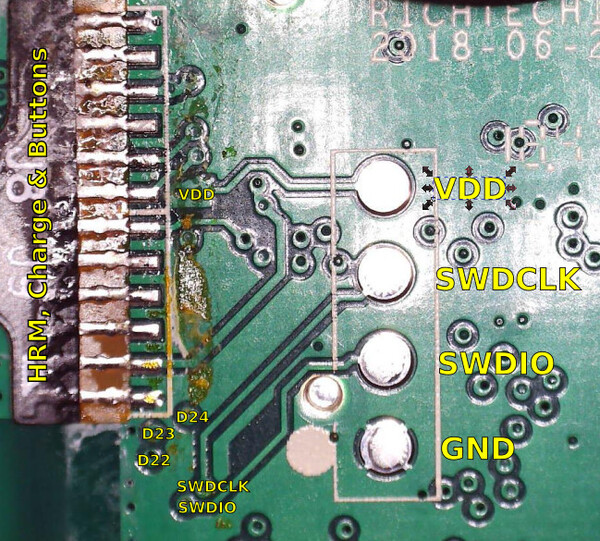
You only need GND, SWDID and SWDCLK (VDD is not required).
See Advanced Debug for more information on programming via SWD.
Heart Rate monitor PCB
On the bottom right of the PCB (by the label R6) are the two
pads for the speaker. The one labelled + goes directly to 3.3v,
and the one next to it goes to pin D18 via a transistor.
As such, D18 is inverted, and can only be used as an output - however
it is powered (pulldown via MMDT3904) so is able to drive reasonably high loads (up to ~100mA).
The heart rate monitor itself is powered from the IO expander, and
has just a single analog output, which is D29.
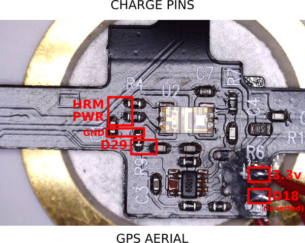
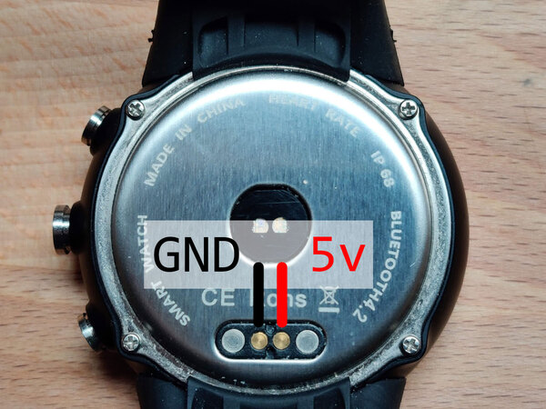
Charging pins
The two circular gold pads interface with the charging circuit. The right-hand
one (with them at the top of the watch) is connected to GND, and the left-hand
one goes to the charging circuitry.
I2C
SCK=D14, SDA=D15
- 0x0C - GMC303 magnetometer
- 0x1E - KX023 accelerometer
- 0x20 - io expander
- 0x7C - Unknown. Only checked once by OEM firmware.
This page is auto-generated from GitHub. If you see any mistakes or have suggestions, please let us know.