STM32L496G Discovery Board
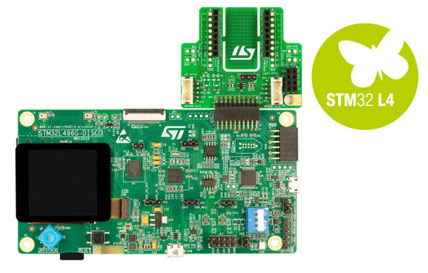
The 32L496GDISCOVERY Discovery board is a complete demonstration and development platform for STMicroelectronics ARM® Cortex®-M4 core-based STM32L496AG microcontroller.
Contents
Features
- STM32L496AGI6 microcontroller featuring 1 Mbyte of Flash memory and 320 Kbytes of RAM in an UFBGA169 package
- microSD™ card connector
- STMod+ and PMOD connectors
- 8 Mbit-PSRAM
- 64 Mbit-Quad-SPI Flash
- 8 LEDs
- Reset push button
- 4 direction-joystick with selection
- USB OTG FS with Micro-AB connector
- Compatible Arduino™ Uno V3 connectors
- On-board ST-LINK/V2-1 debugger
Buying
This board can be purchsed direct from ST or from distributors.
Getting Started
- Plug the Discovery board in via the
USB STLINKUSB connector. - Go to http://www.espruino.com/binaries (or http://www.espruino.com/binaries/travis/master/
for the absolute latest builds) and download the latest file named
espruino_*_stm32l496gdiscovery.bin - Save it to the
DIS_L496ZGdrive that should have appeared on your computer and wait for the LEDs on the board to stop flashing
And you're ready to go! Follow the Getting Started Guide for details
on getting the IDE connected via USB. You can communicate with the board via the
USB STLINK USB connector or the OTG FS USB connector (OTG FS takes priority if connected).
Information
Pinout
Note: All pins on Arduino headers are available via the Nucleo object,
eg. Nucleo.A1.
Hover the mouse over a pin function for more information. Clicking in a function will tell you how to use it in Espruino.
- Purple boxes show pins that are used for other functionality on the board. You should avoid using these unless you know that the marked device is not used.
- ! boxes contain extra information about the pin. Hover your mouse over them to see it.
- 3.3v boxes mark pins that are not 5v tolerant (they only take inputs from 0 - 3.3v, not 0 - 5v).
- GND is ground (0v).
- ADC is an Analog to Digital Converter (for reading analog voltages)
- DAC is a Digital to Analog Converter (for creating analog voltages). This is not available on all boards.
- PWM is for Pulse Width Modulation. This creates analog voltages from a digital output by sending a series of pulses.
- SPI is the 3 wire Serial Peripheral Interface.
- USART is a 2 wire peripheral for Serial Data.
- I2C is the 2 wire Inter-Integrated Circuit bus.
Pins not on connectors
This page is auto-generated from GitHub. If you see any mistakes or have suggestions, please let us know.